PostTime:10/21/2021
After the Scanning Electron Microscope and Focused Ion/Electron DualBeam Microscope, Transmission Electron Microscope (TEM), another new equipment entered the Electron Microscope Center of GTIIT.
How is the transmission electron microscope different from the other two electron microscopes? In what areas will it work? Let's take a look!
Exploring the unknown is the unremitting pursuit of mankind. The use of a variety of instruments and equipment for observation, analysis and research is one of the important means of people to explore the mystery. The transmission electron microscope (TEM) in the Electron Microscope Center of GTIIT is such an efficient equipment to support researchers to carry out interdisciplinary and multi-dimensional research work.
It is Thermo Scientific Talos F200X, which combines high resolution transmission and scanning transmission electron microscope (STEM) imaging with industry-leading energy dispersive X-ray spectroscopy (EDS) signal detection. As an analytical electron microscope, the outstanding advantage of it is that Talos is equipped with the EDS system integrating four silicon drift detectors (SDD), which can maximize the collection efficiency of X-ray and analyze the composition of samples quickly and accurately.
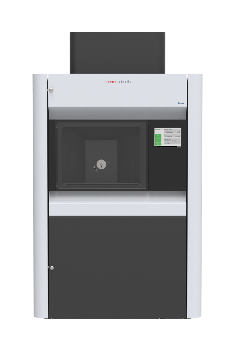
Main specifications
Accelerating voltage: 200 kV, 120 kV, 80 kV
TEM information limit: 0.12 nm
STEM High Angle Annular Dark Field (HAADF) resolution: 0.16 nm
EDS energy resolution: ≤136 eV
Main Functions
High resolution TEM imaging
Bright field (BF) image, dark field (DF) image, atomic image
High quality electron diffraction analysis
Selected area electron diffraction (SAED), nano beam electron diffraction (NBED), convergent beam electron diffraction (CBED)
High resolution STEM imaging
BF image, DF image, HAADF image, differential phase contrast (DPC) imaging
Fast and accurate EDS analysis
Point scanning, line scanning, area scanning
TEM, STEM, EDS 3D reconstruction
Lorentz imaging
Application area
Talos can be applied to multi-dimensional characterization and testing of various materials in the fields of materials science, energy science and life science. The following are some application examples:
AlSi10Mg alloy
Figure (a) is the STEM-HAADF image of AlSi10Mg alloy, figures (b), (c), (d) and (e) show the distribution of Al, Ti, Mg and Fe elements in the sample respectively, and figure (f) shows the overlap of the Al, Ti and Fe elements distribution in the sample.
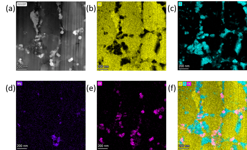
EDS elements mapping of AlSi10Mg alloy
The (111) plane (d=2.34Å), the (1-1-1) plane (d=2.34Å) and the (200) plane (d=2.02Å) under the [01-1] zone axis.
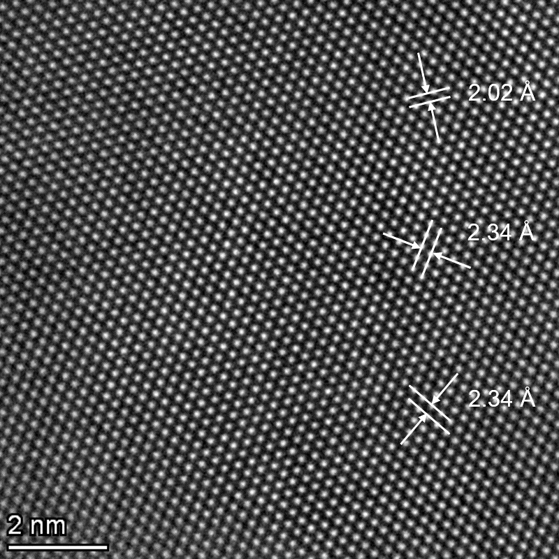
TEM high resolution atomic image of AlSi10Mg alloy
TiAl alloy
The TEM image and the diffraction pattern show the α2 phase and γ phase with lamellar structure in the TiAl alloy, which satisfied the (0001)α2 // (111)γ, [2-1-10]α2 // [110]γ orientation relationship, and there are γ twins in this area.
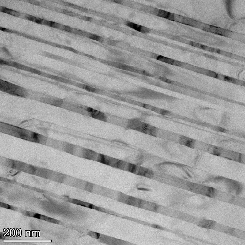
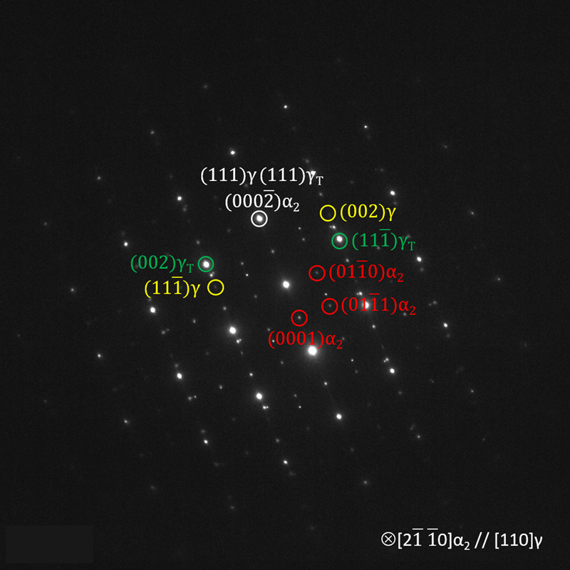
TEM bright field image (figure 1) and selected area electron diffraction pattern (figure 2) of TiAl alloy
Perovskite quantum dots
The atom arrangement in perovskite quantum dots.
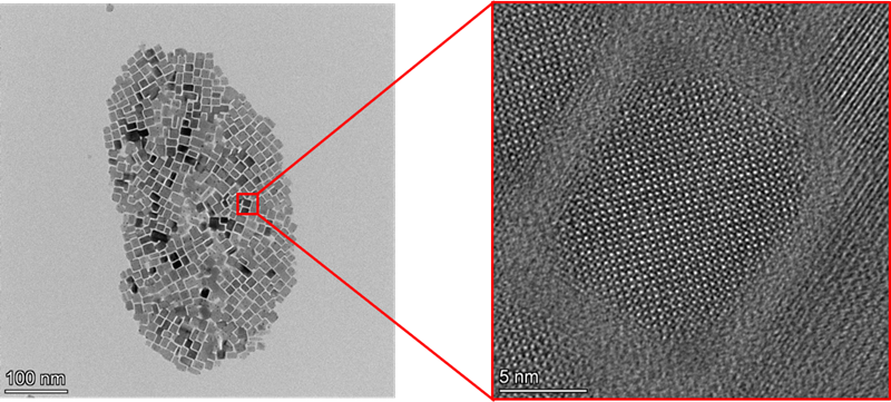
TEM bright field image (left) and high resolution atomic image (right) of perovskite quantum dots
Film
The STEM-HAADF image shows the sharp interface between the film and the substrate, and the distance between atoms of the dumbbell diatomic structure in the upper film is 0.16 nm only.
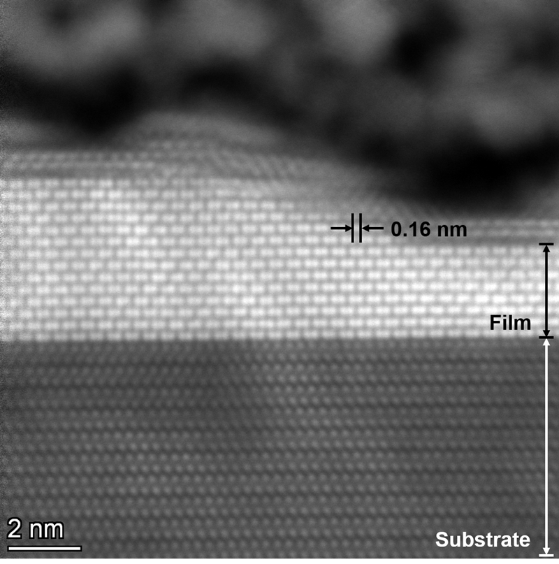
STEM-HAADF high resolution atomic image of the film
Mouse esophagus
The image left shows the normal mouse esophageal epithelium. Mitochondria can be seen in the cytoplasm, and the desmosomes can be seen between epithelial cells. The image right shows the diseased mouse esophageal epithelium. Mitochondria in the cytoplasm disappeared, and the desmosomes between epithelial cells decreased.
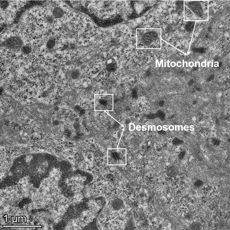
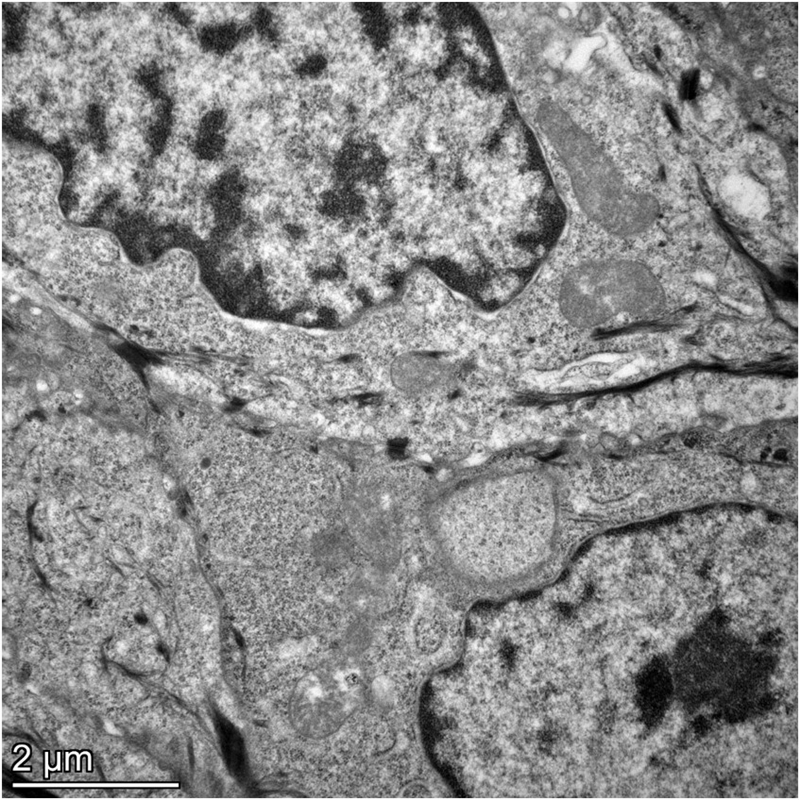
TEM bright field image of normal (figure 1)/ diseased (figure 2) mouse esophageal epithelium
GTIIT Electron Microscopy Center (EMC)
GTIIT has world-class academic environment and research teams. The Electron Microscopy Center (EMC) of GTIIT is an open platform that integrates analytical testing services, fundamental research and applied research. EMC takes the micro characterization of materials as the entry point, studies the microstructure and chemical composition of different materials (up to the atomic level) by a variety of electron microscopy methods, and establishes the internal relationship among the microstructure, chemical composition and material performance, providing basic scientific support for material performance optimization and further application.
Related reading:
Exploration | 微观世界的奇妙探索之旅(一)
https://mp.weixin.qq.com/s?__biz=MzI1NjY0NTMyNA==&mid=2247493497&idx=1&sn=7b65d2afbb4e20fd64d2dc5dfa6ff91d&chksm=ea2126dadd56afcc004953fa4ac6dfe222dc6f655ec7f07648a0e612fe6f490a18e2ab70746d&scene=21#wechat_redirect
Exploration | 微观世界的奇妙探索之旅(二)
https://mp.weixin.qq.com/s?__biz=MzI1NjY0NTMyNA==&mid=2247502781&idx=1&sn=cdbfd27ff78b9e1beeb93430d20872ad&chksm=ea210a1edd56830801733a1e885e0b8e66341de9a858ef1396c2019a0ee56c91e93c7b110b04&scene=21#wechat_redirect
Text/Photos: GTIIT News & Public Affairs, GTIIT Electron Microscopy Center
© GUANGDONG TECHNION-ISRAEL INSTITUTE OF TECHNOLOGY | 粤ICP备17036470号
