PostTime:8/24/2021
The Electron Microscopy Center of GTIIT has added another equipment- Focused Ion/Electron DualBeam Microscope.
How can Focused Ion/Electron DualBeam Microscope serve scientific research? What other functions does it have?
Let's learn more about this Helios 5 UC dualbeam electron microscope.
Have you ever seen the GTIIT logo etched on a silicon chip? Generally speaking, the size that the human eyes can distinguish is 0.1mm, and the size of school badge we can see in the daily life is usually ranged from a few centimeters to dozens of centimeters.
However, the Focused Ion/Electron DualBeam Microscope - FIB, which is designed to process materials in a specific shape, makes it easy to produce school logo tens of micrometers or even smaller. The following figures show the morphology of the school logo etched on the silicon chip by using Focused Ion/Electron DualBeam Microscope.
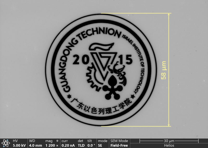
GTIIT badge with 58μm in diameter

GTIIT logo with 180μm in length, 80μm in width
*1cm=10mm=10000μm
This Helios 5 UC dualbeam electron microscope (FIB-SEM) shows very powerful functions and potential. It combines the focused ion column and the innovative electron column with monochromator technology, in addition to its own multichem deposition/ etching system, nanomanipulator, high-precision five-axis motorized stage, sample navigation, plasma cleaner and auto-alignment function, it is also equipped with a variety of detectors. This electron microscope can be used for the fast, easy, and precise high-quality Transmission Electron Microscope - TEM sample preparation and micro-nano processing, and it is also supplemented by electron imaging under different modes and requirements.
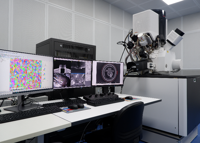
Equipment Introduction
Name:Focused Ion/Electron DualBeam Microscope
Model:Helios 5 UC
Detectors
In-Column Backscattered Electrons Detector (ICD)
Mirror Backscattered Electrons Detector (MD)
Through-the-Lens Secondary / Backscattered Electrons Detector (TLD)
Everhart-Thomley Secondary Electrons Detector (ETD)
In-Chamber Electron and Ion Detector (ICE)
Directional Backscattered Electron Detector (DBS)
Scanning Transmission Electron Mode Detector (STEM)
X-ray Energy- dispersive Spectrometer (EDS)
Electron Backscatter Diffraction Detector (EBSD)
Main Functions
TEM sample preparation
Micro-nano processing
Morphology observation
Compositional, microstructural and crystallographic analysis
3D reconstruction
Advantages
Advanced FIB-SEM dualbeam system and precise sample navigation function enable fast and high-quality TEM sample preparation at specific sites of the material.
The high-throughput ion column can not only mill the samples under high voltage, but also polish the samples with low energy ions to minimize surface damage on the sample.
Equipped with the most advanced software and pattern engine, it is capable of fast, accurate and precise milling and deposition of complex structures with critical dimensions of less than 10nm.
It can provide the highest-quality, fully automated and multi-modal 3D data collection to realize the 3D reconstruction.
The electron column with monochromator technology and multi-detectors can meet high-resolution imaging for different requirements.
Application Areas
It is widely used in the preparation, characterization and analysis of solid materials in many fields such as material science, semiconductor industry and chemical industry.
Functional Application Examples
TEM sample preparation (take silicon wafer as an example, the process is as follows)
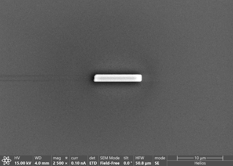
Deposit the protective layer
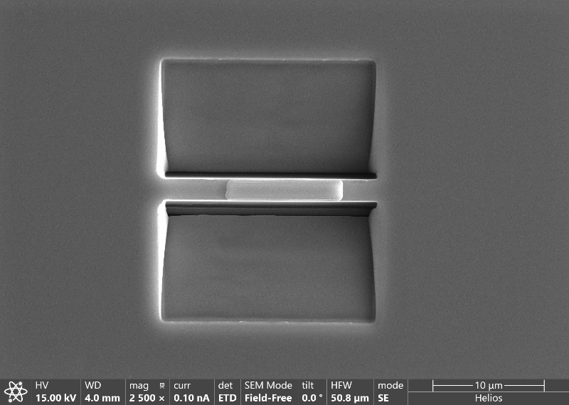
Cut the upper and downer sides
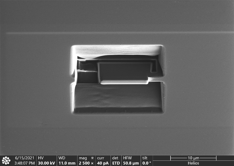
Cut off the left and bottom of the lamellar
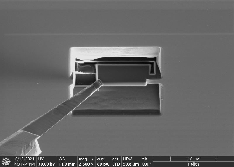
Weld the nanomanipulator to lamellar
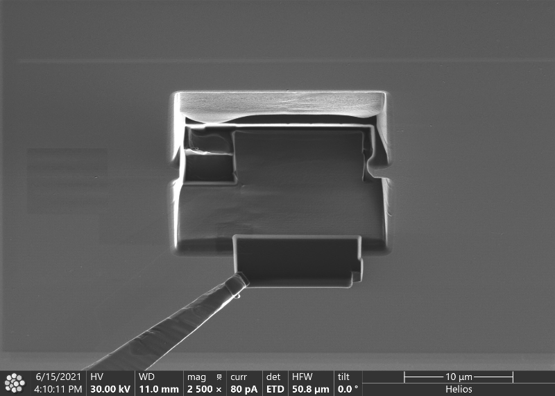
Cut off the right side of the lamellar and take it out
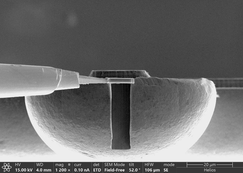
Weld the lamellar onto grid
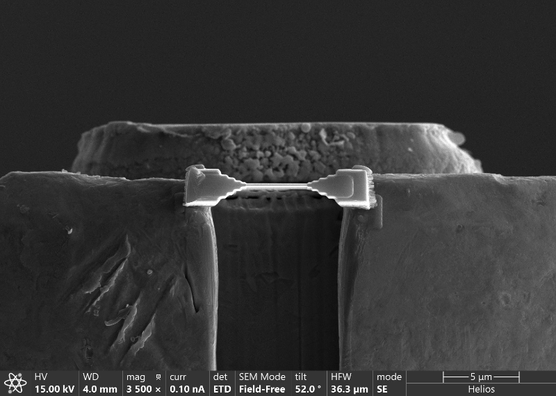
Stepped thinning the lamellar
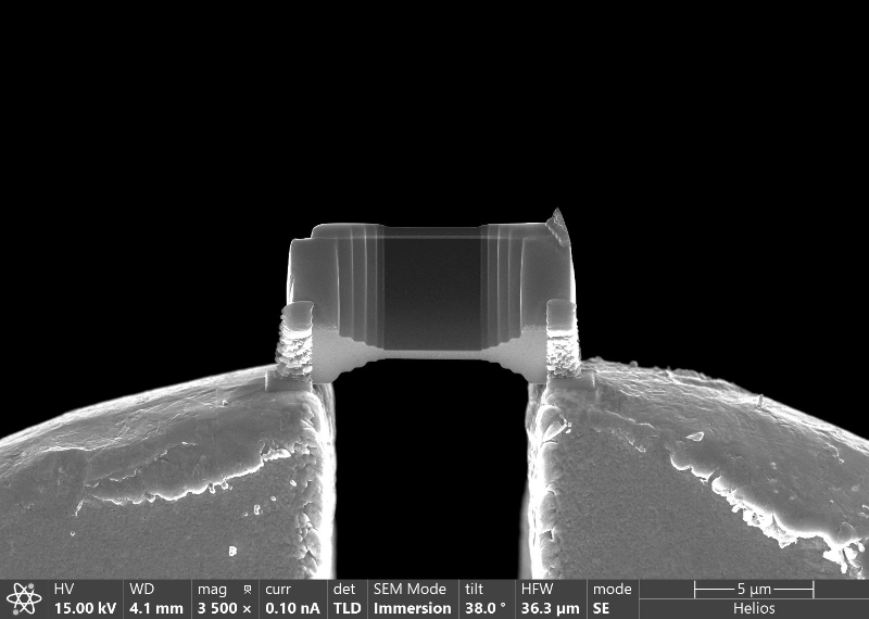
Polish the lamellar
Morphology characterization
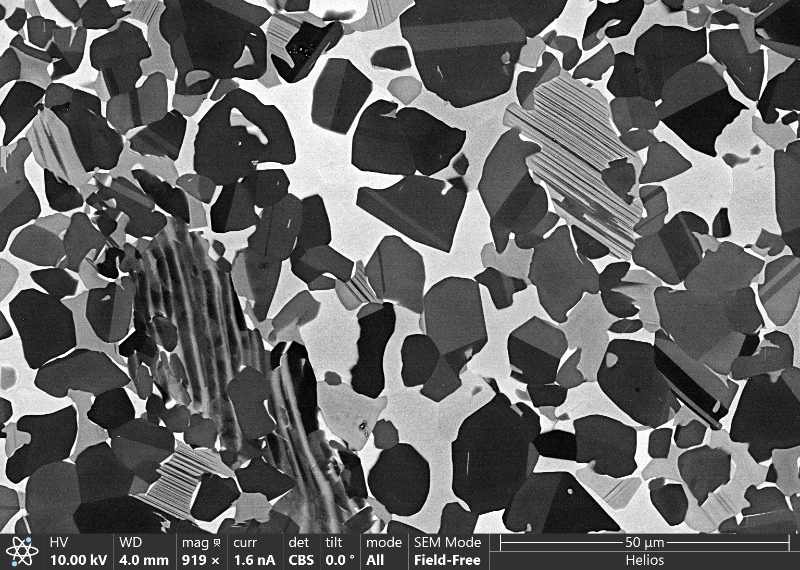
α2、β、γ phases and a small amount of α2+γ lamellar structure in TiAl alloy
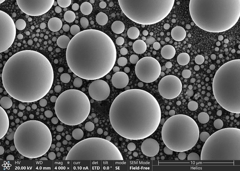
Tin balls in various size
Compositional analysis
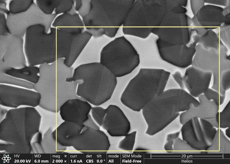
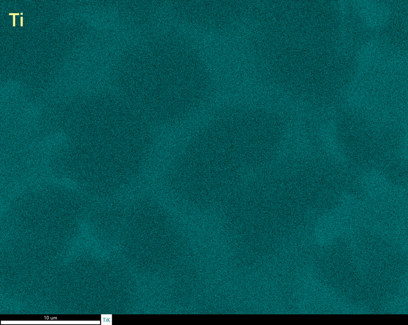
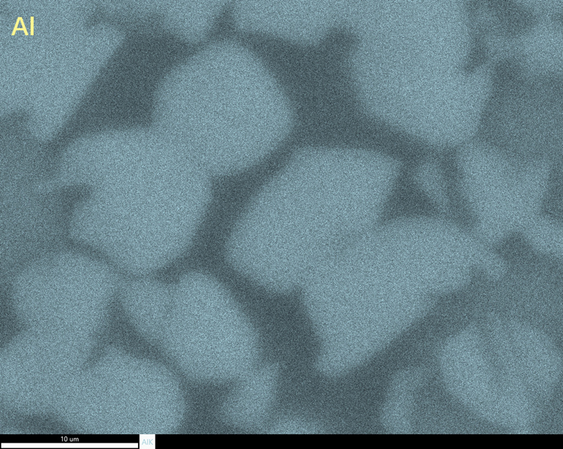
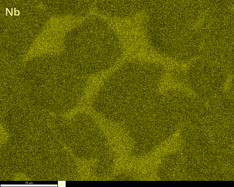
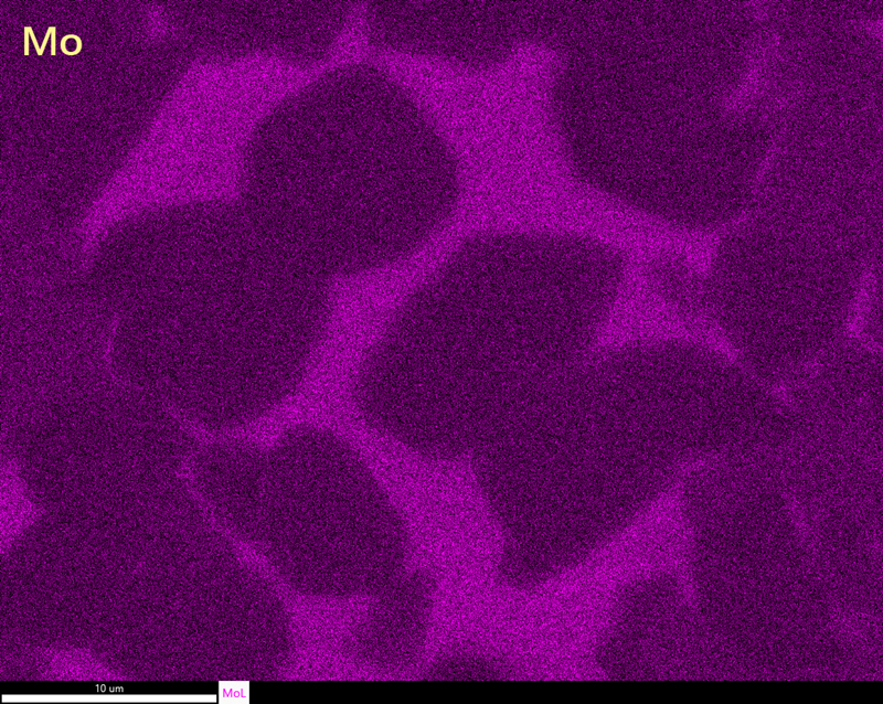
Element distributions in Ti-43.5Al-4Nb-1Mo alloy
Microstructual and crystallographic analysis
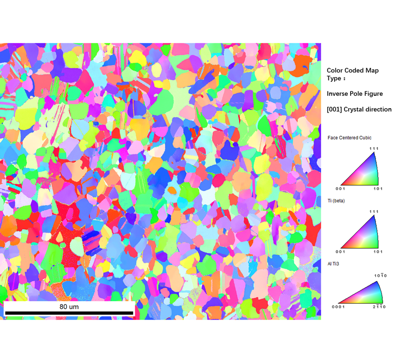
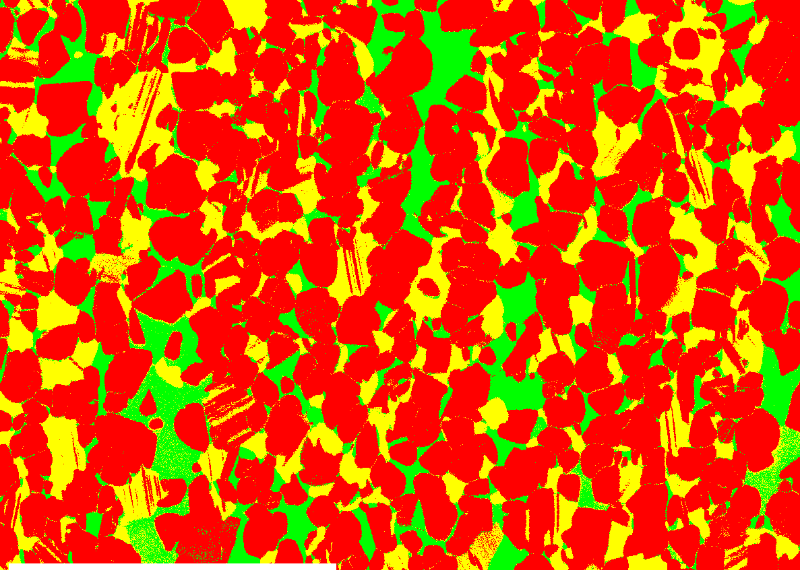
Grain orientations (up) and phase distributions (down) of TiAl alloy
GTIIT Electron Microscopy Center (EMC)
GTIIT has world-class academic environment and research teams. The Electron Microscopy Center (EMC) of GTIIT is an open platform that integrates analytical testing services, fundamental research and applied research. EMC takes the micro characterization of materials as the entry point, studies the microstructure and chemical composition of different materials (up to the atomic level) by a variety of electron microscopy methods, and establishes the internal relationship among the microstructure, chemical composition and material performance, providing basic scientific support for material performance optimization and further application.
Related reading: Exploration | 微观世界的奇妙探索之旅(一)
https://mp.weixin.qq.com/s?__biz=MzI1NjY0NTMyNA==&mid=2247493497&idx=1&sn=7b65d2afbb4e20fd64d2dc5dfa6ff91d&chksm=ea2126dadd56afcc004953fa4ac6dfe222dc6f655ec7f07648a0e612fe6f490a18e2ab70746d&scene=21#wechat_redirect
Text/Photos: GTIIT Electron Microscopy Center, GTIIT News & Public Affairs
© GUANGDONG TECHNION-ISRAEL INSTITUTE OF TECHNOLOGY | 粤ICP备17036470号
