PostTime:10/23/2020
Under the scanning electron microscope, we can see the different structures and morphologies of different materials. Let’s use our imagination and experience the romance of science.
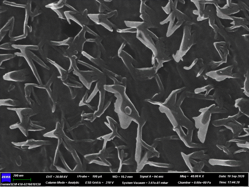
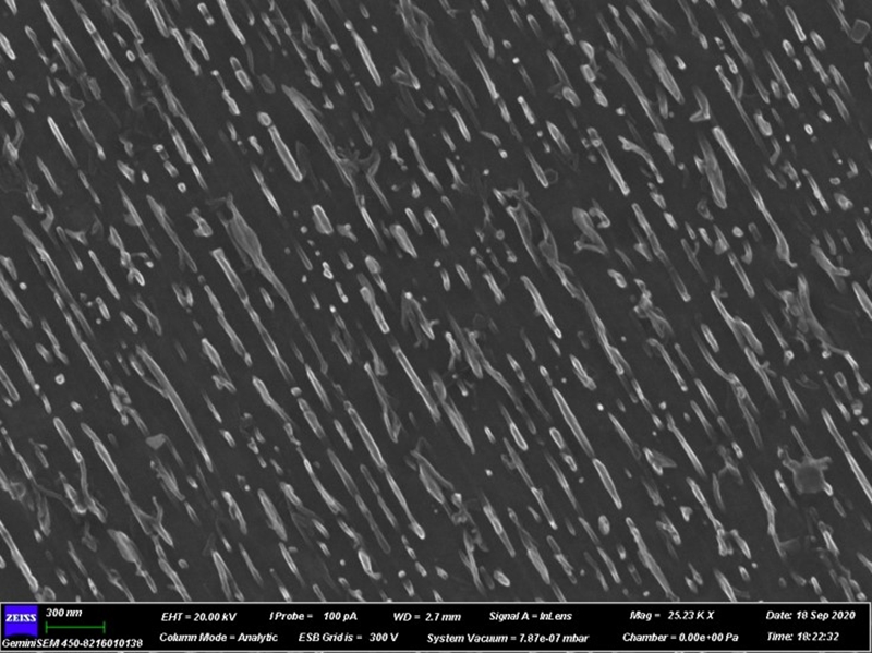
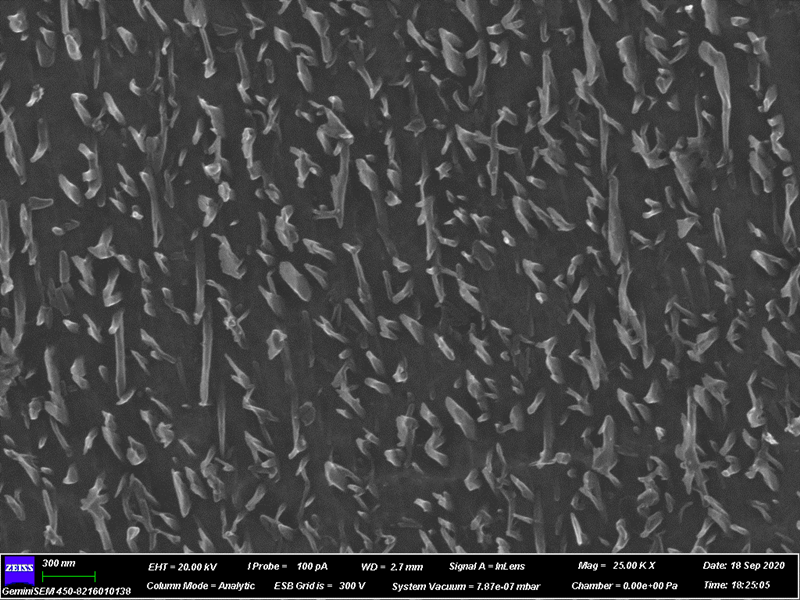
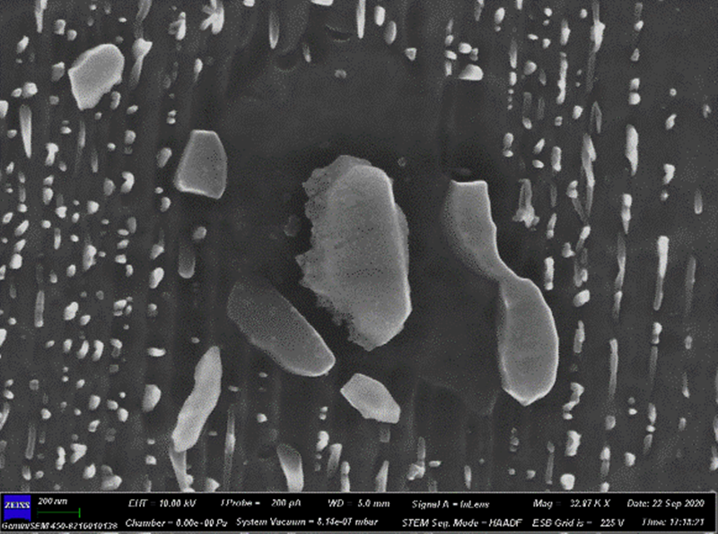
The picture shows the different phases and structures in TNM alloys observed by scanning electron microscope.
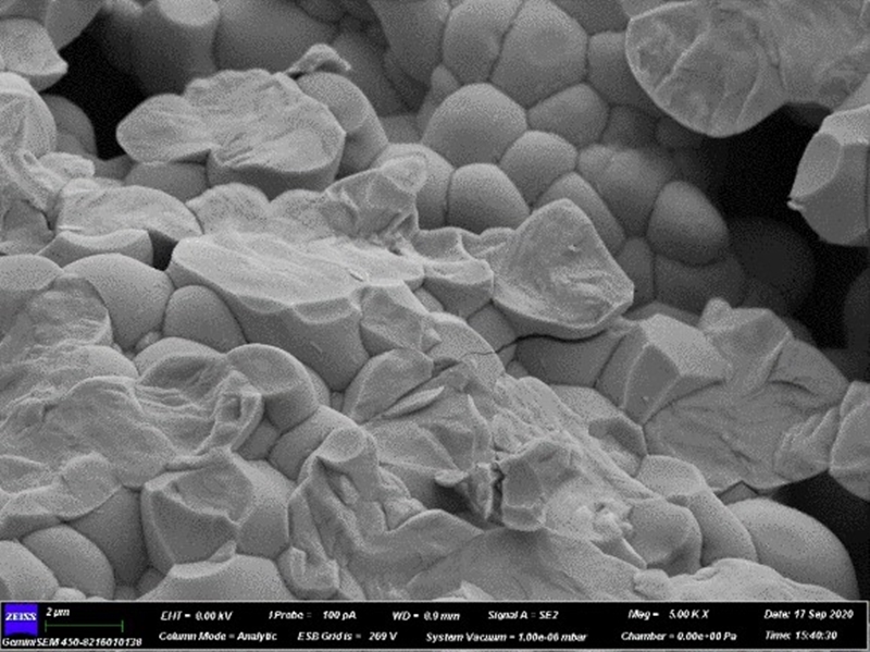
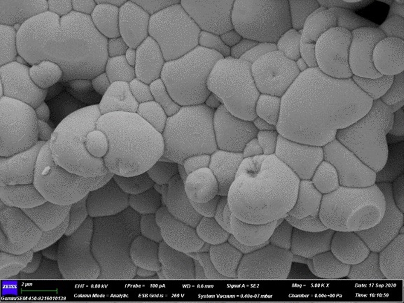
Different fracture morphologies of PZT ceramics
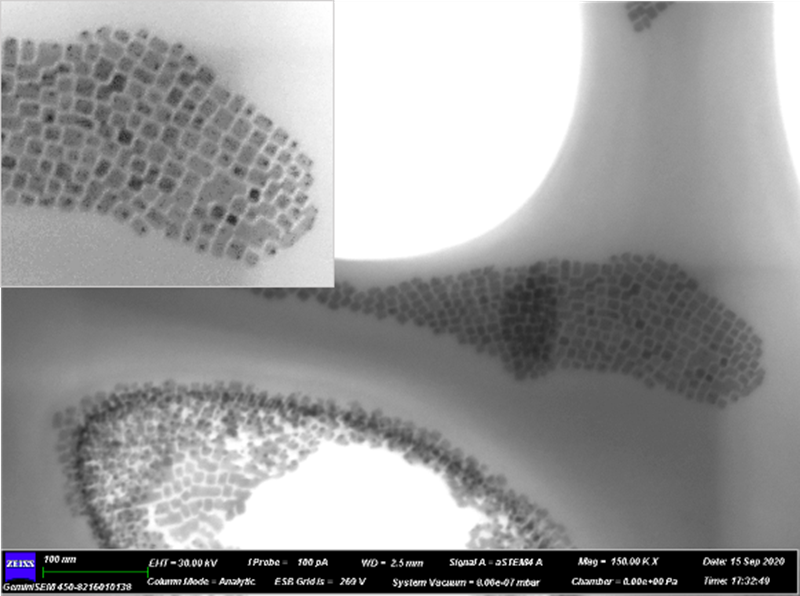
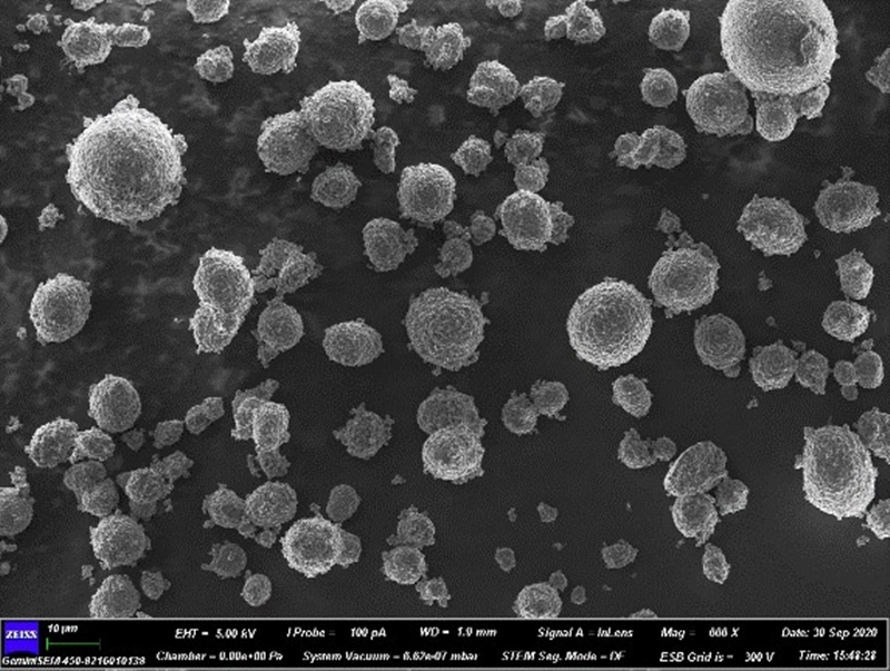
Perovskite quantum dots and Lithium Nickel Manganese Cobalt Oxide
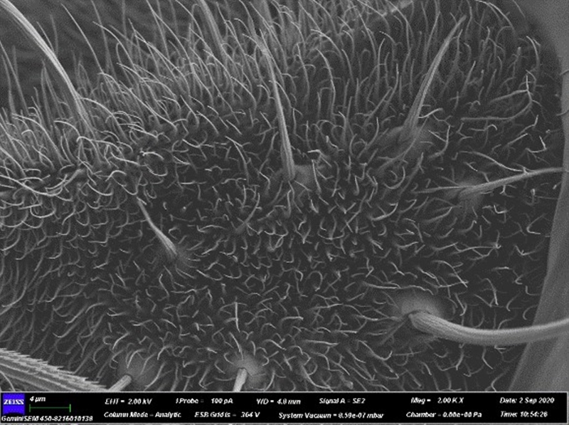
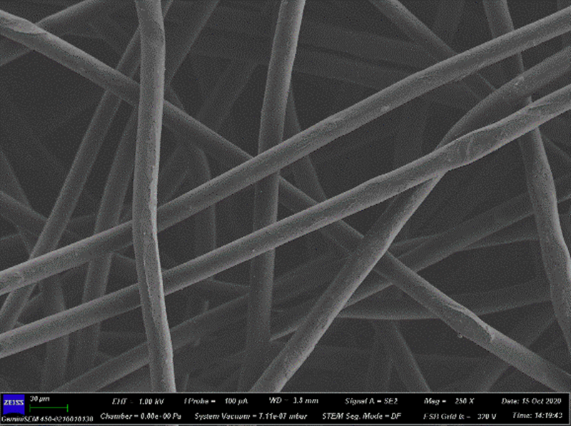
The cilia on a fruit fly and the fibres in medical masks
The interesting pictures above are all from the scanning electron microscope (Zeiss GeminiSEM 450) at the Electron Microscopy Center of GTIIT.
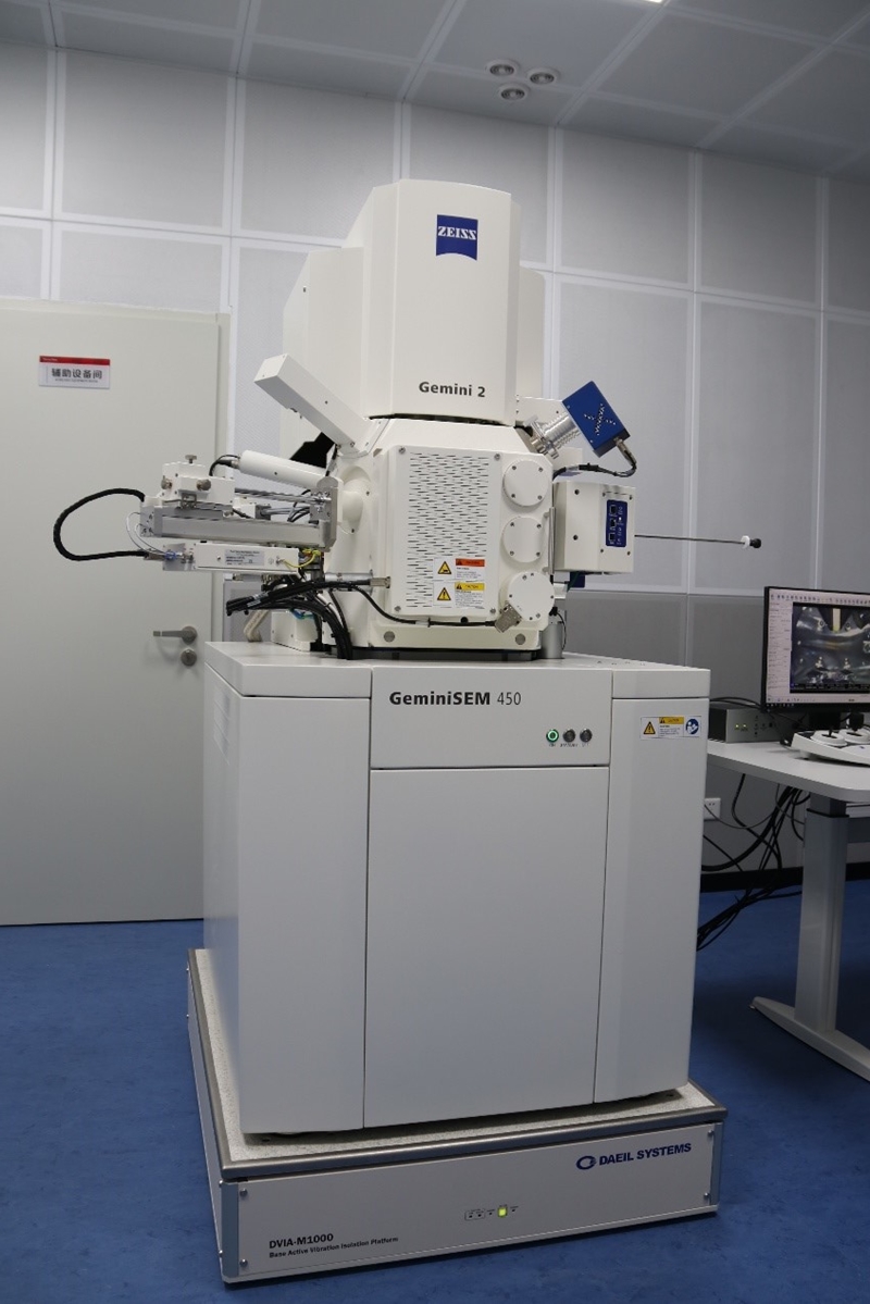
Main application areas
High-resolution topography observation
Failure analysis of semiconductor materials
Material composition and crystal structure analysis
Host configuration
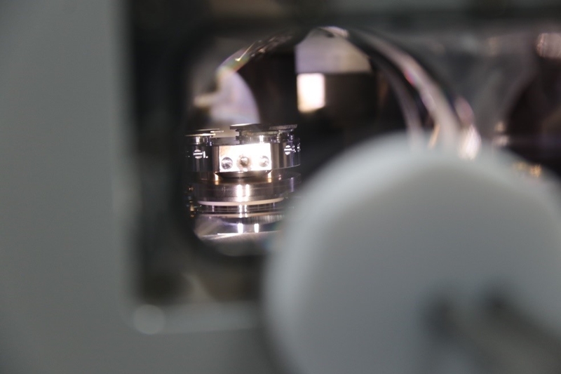
In addition to Gemini2 Double Condenser Electron Optical Tube, 80 mm sample exchange room and plasma cleaning instrument, the device is equipped with seven detectors for different modes.
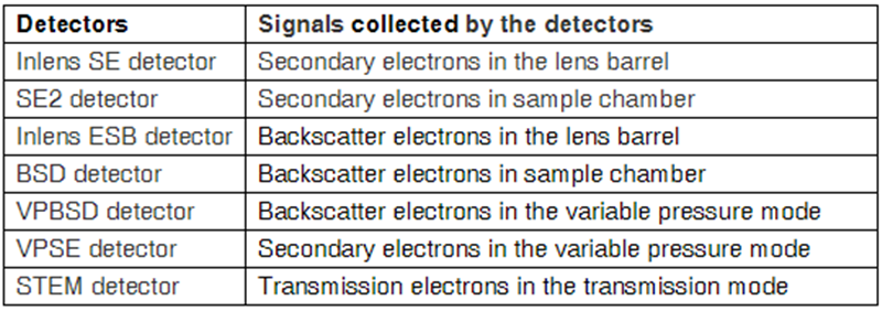
Advantages
No magnetic flux leakage objective lens design, which can perform high-quality imaging of challenging samples such as weak magnetic materials.
Various detection modes, in variable pressure mode, it can image almost any type of samples, such as electron beam sensitive samples, samples without conductive coating, etc.
The acceleration voltage is continuously adjustable in the range of 0.02~30kV, and the probe beam current is continuously adjusted in the range of 3pA-40nA. According to the characteristics of the sample, it can freely choose the appropriate voltage and beam combination for imaging and analysis. The resolution can reach 0.7nm at 15kV acceleration voltage.
Seamlessly switch between low-beam high-resolution imaging and high-beam analysis mode. In addition, it can be equipped with an energy spectrometer and a backscattered electron diffraction detector for material composition and crystal structure analysis.
Introduction of the Electron Microscopy Center (EMC) of GTIIT
GTIIT has world-class academic environment and research teams. The Electron Microscopy Center (EMC) of GTIIT, which is currently under construction, is an open platform that integrates analytical testing services, fundamental research and applied research. EMC takes the micro characterization of materials as the entry point, studies the microstructure and chemical composition of different materials (up to the atomic level) by a variety of electron microscopy methods, and establishes the internal relationship among the microstructure, chemical composition and material performance, providing basic scientific support for material performance optimization and further application.
Aims and Instruments
Research fields of the EMC include materials science, condensed matter physics, energy, nanotechnology and the cross-discipline of technology. It mainly consists of high-end instruments: Transmission Electron Microscope (TEM), Focused Ion Beam system (FIB), Scanning Electron Microscope (SEM).
Developments
Currently, the SEM has been settled in the Electron Microscopy Center, now it is in the debugging stage and will be open for use soon. TEM and FIB will be installed in the center this year.
Demonstration Cooperations
At present, GTIIT Electron Microscopy Center has cooperated with Zeiss to establish a scanning electron microscope demonstration laboratory, and another demonstration laboratory cooperation programs have been established with Thermo Fisher and Ametek, respectively. GTIIT Electron Microscopy Center is the highest electron microscopy analysis platform among the universities in the Eastern Guangdong Province.
Team Members
The team of the GTIIT Electron Microscopy Center is composed of Limei Cha (the second row left), Director of Electron Microscopy Center, and three experienced electron microscope engineers including Jingfang Shen (front row left), Wenjing Zhang (front row right), and Zhixiang Si (second row right).
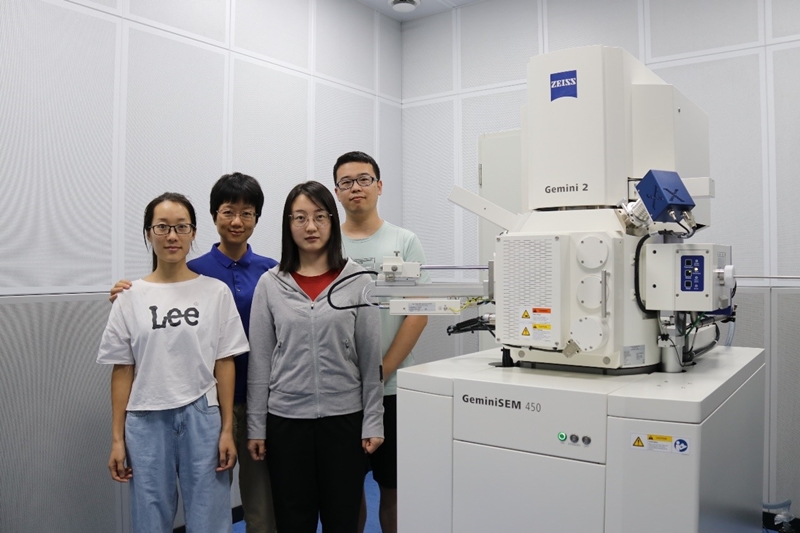
Limei Cha is the Director of the Electron Microscopy Centre, who graduated from Max-Planck-Institute for Metal Research in Germany. Her tutor is Professor Manfred Ruehle, a famousexpert in transmission electron microscopy and academician of German Academy of Sciences. She has solid theoretical knowledge foundation and rich practical experience in the field of microstructure and electron microscopy analysis of materials. She engaged in materials analysis and research for more than ten years, working in the electron microscopy team of the best national laboratories in Europe such as Germany, Austria, France, etc., and communicating and cooperating with top teams at home and abroad. After returning to China, she was independently responsible or cooperating with others to complete 7 national or provincial natural science fund projects. She joined GTIIT in mid-2018 and started to planand build GTIIT Electron Microscopy Center.
The three electron microscope engineers have studied or worked in Harbin Institute of Technology, Zhejiang University, Shandong University, Beijing University of Technology, Taiyuan University of Technology, China Aviation Development Guizhou Liyang Aviation Power Co., Ltd.. They have solid theoretical basis and rich practical experience in electron microscopy, and can skillfully use and maintain multiple types of electron microscope.
Text: GTIIT News & Public Affairs
Photos: GTIIT Electron Microscopy Center, GTIIT News & Public Affairs
© GUANGDONG TECHNION-ISRAEL INSTITUTE OF TECHNOLOGY | 粤ICP备17036470号
